
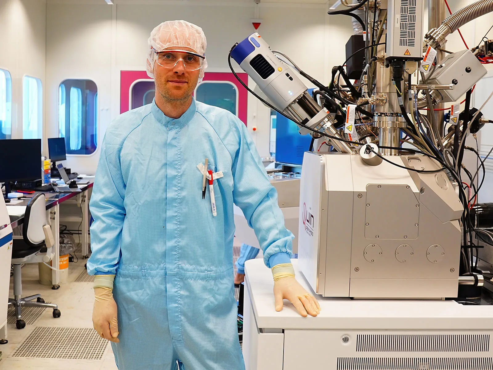
“We set out to build more than just another cleanroom.”
Jakob Buchheim,
Head of Cleanroom Laboratory Operations at the DLR QCI
Jakob Buchheim had been fascinated by working in cleanrooms for a decade before he took on his biggest challenge: building a user facility for highly specialised deep-tech start-ups at our Innovation Centre in Hamburg.
Jakob, let’s start with a silly question: Are all cleanrooms the same?
No, of course not! The term ‘cleanroom’ is often used in a very general sense. But in reality, it involves many technical details and specific decisions. To build the cleanroom in Hamburg, we had to understand what was actually required. This is where the details matter and one of the biggest challenges, especially at the start, when it is not yet clear what companies want to achieve in concrete terms.
What were the constraints you had to work with?
Basic framework conditions, such as fire protection, were already covered by the building’s existing infrastructure. At the same time, the limited space was the real challenge. It turned the planning process into something of a puzzle and made it highly demanding.
When designing a cleanroom, you want it to cover the entire process chain: from the starting substrate – for example, a silicon wafer or glass wafer – right through to the finished component. It is not enough to carry out only some of the necessary processes on site and outsource others. The individual process steps and materials are too closely interdependent. Outsourcing would also result in considerable waiting times and organisational overhead. That is why the entire process chain must be available within the cleanroom and carefully coordinated. In the end, we had to integrate 35 specialised systems. This enables us to cover the entire process chain.

What makes a good cleanroom team?
For a project of this scale, you need people who are willing to fully commit to the task under the given conditions and take responsibility.
We were very fortunate with the appointment of the laboratory management team. They embraced the challenge and the responsibility with great commitment and have been steadily building up the Hamburg team since March 2023. They are supported by technicians and process engineers who are gradually commissioning the systems, operating them and further developing the manufacturing processes. The team also includes technical assistants responsible for plant technology and building interfaces, two process engineers who develop and supervise systems and processes, and a researcher who supports companies, in particular, with consultancy and the integration of processes across entire process chains. In addition, four team members share some responsibility for machine operation whilst managing their technology development projects.
Overall, we now have a highly capable operational team that successfully manages and continues to develop the cleanroom. One of our strengths is our interdisciplinary approach. We have engineers from various disciplines, materials scientists, electrical engineering specialists and physicists. This diversity is essential for developing microtechnological systems and processes for quantum systems. It also facilitates collaboration, as we, other researchers and companies often bring different perspectives and specialist terminology to the table we share with many start-ups.
And what brings you together?
A fascination with microtechnology: manufacturing structures with the utmost precision – structures that are often only visible under a microscope in the end. We also all feel that we are contributing to something new – something that could really make a difference. There is no set formula; we are working on a highly innovative integrated system in which many aspects still need to be developed. That creates a strong bond within the team.
When you built the cleanroom, did you simply meet the requirements of the partner companies?
Well, it wasn’t quite that simple. During the contract and procurement process for the DLR QCI’s quantum computers, the companies were able to put forward requirements for the DLR infrastructure and, consequently, for the cleanroom as well. However, for some of the companies – often young start-ups within the DLR QCI – the process was more of a learning experience. Together, we developed suitable process chains and boundary conditions and assessed whether these would be viable for the companies.
Other companies faced patent-related constraints, as certain process details or technologies for producing surface structures are protected or confidential. Consequently, they were unable to provide all the information we would have required.
In practice, this meant that we had to develop a coherent overall concept from very different starting points and derive concrete process plans from it. A great deal of interpretation and design work therefore fell to DLR.
Will further expansion of the cleanroom require more systems, more staff, or both?
The cleanroom is clearly needs-based. At its core, it is about solving specific problems for companies and enabling them to carry out their work. If demand increases, we can respond accordingly. The investments in the infrastructure have already been made, so the basic foundation is in place. The key factor is therefore staffing. If more specialists are available, more processing technologies can be offered and significantly more users and companies can be supported.
But that is not easy. We are talking about highly specialised micro-production systems that require constant supervision. On average, a process engineer should spend around one to two days a week on each system to ensure its operation, process stability and further development. That means one person can realistically supervise no more than five systems to the required standard.
We deliberately chose our current approach. The aim is not to provide as many resources as possible, but to operate the available systems with the necessary technical expertise and quality. Particularly when it comes to complex microtechnology processes, intensive support is a key factor for success.
What systems and tools do you use?
A key element in the microproduction chain is patterning, which refers to lithography. For this, we use two established methods. The first is a laser lithography system, which transfers a design directly onto the substrate. Think of a rapid prototyping system or a 3D printer. What is important here is a sequential yet rapid writing process that enables us to produce structured wafers efficiently. The second is UV lithography, particularly for larger production runs. For ion-trap applications, nanometre-scale structures such as those found in conventional computer chips are not required. Micrometre dimensions are entirely sufficient. This combination of laser and UV lithography is therefore a well-established and suitable cleanroom standard.

One particularly specialised system is the electroplating unit. It enables the deposition of very thick metal layers, which are required for the conductive structures of ion traps. These layers are essential, but electroplating systems of this kind are not found in every cleanroom.
Another specialised system is a cryogenic wafer prober. It allows us to test components under realistic operating conditions, similar to those they will later encounter in an ion-trap quantum computer. For metallisation, we also have two additional methods available: an evaporation system and a sputtering system. Both are used to deposit metal films, but they differ in their physical properties and therefore also in the resulting material properties, such as crystal structure or homogeneity.
How are the individual steps in this process chain linked?
Take thermal effects on materials, for example. If a metal has been deposited by electroplating, the substrate can often only be exposed to temperatures below around 150 degrees Celsius afterwards; otherwise, the material properties may change. We have to take such interactions into account in the overall process design.

That is precisely why the individual system is not the only decisive factor. What matters is the interplay within the ‘flow’, that is to say, the entire process chain from substrate to finished component. We want to develop stable and reproducible processes, for example for conductive layers, insulating layers or precise electrode structures.
Is this just one cleanroom amongst many?
I believe our cleanroom in Hamburg is quite special. In 2025, the EU made a specific investment decision under the Chips Act and launched a Europe-wide call to develop a pilot line for the production of ion traps. Around 45 million euros were to be provided. When I read that, my first thought was: in principle, that is exactly what we already have. And it shows just how important this kind of infrastructure is. Traditional chip manufacturers are structured in such a way that they do not constantly alter stable and highly optimised processes. Their processes often cost millions and are therefore not designed to deal with experimental materials or new phenomena such as motional heating in ion traps.
What is motional heating in ion traps and why is it important?
Motional heating in ion traps refers to unwanted heating effects in trapped ions, which are thought to depend heavily on the material, surface structure and manufacturing process of the metal layers. The exact causes have not yet been fully investigated, but the DLR QT-IMN team is working on them.
For questions such as these, there is as yet no established market within the industrial sector. And that also means there is no suitable production infrastructure – no environment in which new technologies can first be developed, tested and iteratively improved. So, we take the technological basis and adapt it to new physical systems and requirements. But this is not a simple transfer. It is more of an evolutionary process, because many processes are not directly compatible. This is precisely where gaps emerge – gaps that require specialised pilot lines.
And can you bridge these gaps?
Exactly. We want to provide an infrastructure that is specifically designed as a user facility for companies, enabling them to further develop their technologies whilst outsourcing complex process development. This applies both to the ion traps in Hamburg and to our activities in Ulm, where we have established a similarly specialised infrastructure in the field of diamond-based quantum systems.
In both cases, the key feature is the combination of highly specialised microtechnology, a targeted focus on quantum systems and an infrastructure model that is deliberately positioned between a research institution and an industrial development platform.
Why don’t companies simply build their own cleanrooms?
Because it is far too expensive. In Hamburg alone, we are talking about investments of around 30 to 35 million euros to build this infrastructure. That is a scale that is hardly feasible for start-ups. Even with venture capital, such a set-up would hardly make sense, because it does not directly serve the actual business case. Initially, it merely creates infrastructure. Furthermore, a single start-up would usually be unable to make full use of this infrastructure.
That is why our approach is not to build this infrastructure separately within individual companies, but to provide it centrally as a shared cleanroom facility. Companies therefore do not have to bear this high barrier to entry themselves. Instead, they can access a shared platform to further develop their expertise.
Do other providers do this as well?
Leading German players in the field of microtechnology often operate on a contract manufacturing model. The processes are defined, carried out and then delivered by external parties. This is a completely different model from our user facility.
Our approach is more collaborative. Companies work directly in the cleanroom, further develop processes together with us and build up their own expertise. This is particularly crucial at an early stage of innovation, for example in quantum systems. Many companies are not yet able to specify their processes in sufficient detail, or they deliberately choose not to disclose detailed process knowledge. This is the niche we serve: not merely providing a service, but joint development.
Could universities not fulfil this role?
University cleanrooms are often highly project-driven and dependent on individual PhD projects. As a result, there is often no overarching view of complete process chains and their stability. Our aim, by contrast, is to develop and document processes in such a way that they can be transferred to other settings. Once a method is proven to work and is stable, it should be described so clearly that it can also be reproduced in other facilities, such as an industrial foundry.

The key point is this: the transition from ‘it worked once’ to ‘it is reliably reproducible’ is extremely demanding and often requires more resources than the initial demonstration itself. But it is precisely this scaling-up and stabilisation phase that is crucial for companies if they wish not only to demonstrate products once, but to manufacture and sell them reliably over the long term. In that sense, we act as a bridge. We develop processes in collaboration with companies to the point where they can be transferred to industry, without becoming a foundry ourselves.
But does that not mean that innovation remains dependent on public funding?
For me and my team, the next clear milestone is companies saying: ‘This cleanroom and the processes you offer here are worth contracting.’ That would not only validate our work, but also be an important step for the entire ecosystem.
Many companies in the field of quantum systems – whether sensors or quantum computers – are currently still highly vertically integrated. They develop everything themselves, from the chip to the software, and have to maintain expertise across many areas simultaneously.
I do not believe this model is viable in the long term. A sustainable ecosystem can only emerge when specialised partners work together.
We, as experts in microtechnology, provide stable processes and development support, whilst the companies can focus on their core competencies. A positive sign for us would be companies being able to develop chips and processes with us with relatively little overhead, trusting our expertise and focusing their own resources more strongly on design and system development. After a certain development period, they could then take their IP and have it mass-produced by an industrial manufacturer. We would act as an incubator and development partner within an innovation cycle that later transitions into industrial production.
And then you’d run out of work?
No, quite the opposite. Scaling is still at a very early stage, and particularly in ion traps, many future problems will be deeply rooted in microtechnology. Current systems are being developed with fewer than 100 qubits. In the coming years, we will be looking at systems with hundreds of qubits. This will create entirely new technological challenges, because as the number of qubits increases, so does complexity. Larger systems require many electrodes and voltage sources that have to be integrated and controlled. Classical external control quickly reaches physical and technical limits in this context.

That is why it will be necessary to integrate more logic and control directly onto the chip in order to keep this complexity manageable. Similar challenges also exist in optical control, for example in the integration of waveguides for laser manipulation. This means that even if the ecosystem develops successfully, there will still be a great need for innovation. With the infrastructure we have now built, we can play an active role in shaping how these next-generation challenges are addressed.
Do other fields of research also benefit from your findings?
In the field of quantum systems, there are strong synergies between quantum communication, quantum sensing and quantum computing. This is mainly because the field as a whole is still at a relatively early stage of development, and many of the underlying technologies can be applied across different applications. For us, this means that we are building shared technological expertise that can be flexibly applied to different applications depending on the development path. Many of the underlying processes and materials can therefore be utilised in different quantum technologies.
One concrete example is the integration of hard magnetic layers. These were originally investigated in the context of ion traps on silicon and yielded good results there. During discussions with partners, it then became clear that the same process could also be applied to diamond systems and provide significant added value there as well. This is how a single technology can give rise to several avenues of application.
How does a shared cleanroom like this pay off?
First of all, a major advantage of the DLR QCI is that there was no need to build several separate cleanrooms. Instead, a single shared infrastructure is utilised. This not only significantly reduces investment costs, but also brings together personnel, know-how and technical expertise in one location. Through the shared use and development of the infrastructure, the participating companies also benefit indirectly from the experience and expertise that is built up – naturally without any direct transfer of intellectual property. Overall, pooling these technological capabilities leads to more efficient development than would be possible in isolated individual projects. It creates an environment in which the technological foundations for different quantum systems can be jointly developed and advanced. This brings clear advantages in terms of efficiency, speed and knowledge building.
And is there no competition between the actors involved?
To begin with, we share a common vision and are constantly exchanging views on which challenges need to be tackled first. Precisely because we are operating in a nascent industrial sector where requirements are sometimes not yet clearly defined, this collaboration is crucial. By defining our challenges together, we raise the profile of the entire sector. This has a direct impact on suppliers and manufacturers of peripheral equipment, as it enables them to align with development cycles and develop solutions tailored to these specific requirements from the outset.
The real driving force lies at a meta-level. By bringing together stakeholders facing similar – and in some cases competing – challenges, a clearer picture emerges of what is technically required. For individual stakeholders, it would often not be attractive enough to develop solutions. But once it becomes apparent that several partners share the same need, market incentives can begin to emerge. In my view, this effect is crucial if a genuine industrial sector is to develop: specialised players developing solutions for other specialised players, rather than everyone trying to cover the entire value chain on their own.


